

Hello All ,
In this thread I will present tool which is designed especially for researching and developing many devices threated here on the forum. It consists of three different modules(for the moment), and is very flexible. Many different topologies of switching can be easily assembled by combining the modules in different ways and with different setups and configurations. The signal source is a two phase PWM module with combined analogue and digital features. It is based on an enhanced 8bit MC, the PIC16F785 with specific peripherals, like a dual phase PWM module and two hi speed comparators, which are used for analogue duty cycle adjustment with infinite resolution. To overcome the limited period resolution typical for digital PWM devices, an adjustable external oscillator is used to clock the MC, which in combination with the pre-scaler allow an infinite period resolution over a wide range of frequencies as well. The second module is the switchboard, which is designed as single floating switch, which allows to assemble simple Hi or Lo side pulsing, half bridge or full bridge topology, or floating coil shorting as well as multiple other configurations as required.
The third module is the floating driver power supply, which provides a galvanically isolated supply for various switching drivers. In the thread we will discuss different solutions for specific applications. Schematics , images and videos on the development will be released as well as firmware and software solutions for specific requirements.
Developing a modular switching tool for Research
- 4.5K Views
- Last Post 24 October 2021
- Liked by
-
-

-

-

- and 8 others

In a first stage I nave build the Two Phase PWM circuit on stripboard and test to find the appropriated values for the discrete components and work out the source code. For the moment the work and progress will be posted here, participation and suggestions are welcome as always. The tool resulting from this work it will be released as open source, for those who wish to build it, and readymade modules and tool kits will be available for order soon, part of the incomings will return for support the forum. This first schematic is a draft, to be improved while developing and testing is going on.
Edit:Some additional data about the basic operation of the device: the components in the rectangle at the right side RV4 R4 C5 are the external adjustable clock for the MC.RV1 D1 C4 makes a sawtooth generator for the timing of phase 1 duty cycle, same as RV2 D2 C3 for phase 2. When the output signal of the respective phase goes hi the capacitor charges up until the comparator reaches the reverence value and terminates the pulse.RV3 R3 are for a coarse adjustment of the reverence voltage for both comparators, this is necessary to set properly the value for different frequency ranges. The Dip switch is to configure the frequency range by system clock dividers and shift value between the phases. With the Sync Signal available on J5 another MC can be synchronized for example to use a synchronous rectifier with certain time delay. On J4 two additional GPIO ports are available for sensing purposes.

The signals can be configured as free running two phase signal with independent adjustable duty cycles, or as complementary drive signals for half or H bridge topology with programmable deadtime or overlapping. A synchronization feature allows to connect various MC in parallel in order to add more phases if needed.
- Liked by
-
-
-
.jpg?width=20&crop=0,0,20,20 "fer123")
-

- and 3 others
I have simplified the circuit, reducing it to only the two phase signal source, the other features will be available on the definitive PCB for optional use. Anyway to make the circuit operational a PIC programmer is needed, so also the programmable configurations of the MC can be set up this way, simplifying the basic circuit considerably.
I have built this circuit for first testing: 
A connector socket for the PIC programmer has been added, and all additional(optional) circuitry removed. Some component values might need to be modified to match the required frequency and adjustments ranges, I'm still waiting for some components for final adjustments.
here a video from the first test:
Vidura
- Liked by
-
-
-
-
- and 2 others

In this place I would like to share some experiences of my own regarding the signal source. In the beginning I worked with basic equipment only, a 555 PWM circuit with duty cycle adjustment and a other digital PWM built with a PIC micro. I had some good results with the analogue 555circuit, as it is possible with two potentiometers adjust frequency and duty cycle at the same time, and analogue devices have the advantage of infinite resolution, this can really make a difference when dealing with very narrow values for the sweet spot of a device. In all conventional digital PWM circuits there is a kind of rippling, due to the own clock frequency of the MC, this limits the outputted signals to be always harmonics to this processor clock. This can in some cases make devices fail to get properly tuned. Anyway the 555 circuit has its drawbacks and limits as well. Later I bought a SG, not the best but quite useable , a good tool for many things, but not nearly close as good for most pulsing experiments as the analogue device. Too much time turning the encoder wheel, pressing switches , changing ranges , and modes. It might take you an hour to find a specific spot of tuning, wich can be don in a few minutes with the analogue source. But there is no doubt that MCs have many advantages, and are more stable as a 555timer circuit. MCs are programmable and can manage lot's of tasks, they are very flexible devices. So I was looking at a solution which combines the most important features of both technologies. The result can be viewed in this thread.
Regards Vidura
- Liked by
-
-
-
-

- and 2 others
The floating Driver power supply:
In order to maintain all connected switches floating and galvanically isolated I designed this power supply, capable to feed four drivers on different switch modules:

EDIT: here the revised version
Note that some of the posted schematics are still drafts, so if you decide to build some of the devices please be patient, when they are updated with correct values I will replace them and put versioning f. ex. Driver power supply v1.0 when approved, v0.x means a draft!
- Liked by
-
-
-
-
- and 3 others

Hi Vidura,
Excellent work and a very insightful approach (imho)!
Good luck; have a great week; and Happy Mothers Day to your "Commander and Chief!"
SL
- Liked by
-
-

-

The power switch module:
For greatest flexibility the power switch module is designed as simple switch unit, with an optical insulated MOSFET-IGBT driver, and integrated voltage regulator and filter for the driver supply.
And here a Switch modul with handcrafted prototype PCB version1:

version2, after some layout corrections:


- Liked by
-
-
-
a first switching test of some interconnected modules:

Really very happy with the optical drivers, 100ns fall time is not bad at all!

Here a Block diagram for a H bridge example:
The switch modules with the driver power supply can be fed safely by other signal sources, like SG or Arduino board, thanks to the opto isolated drivers.
- Liked by
-
-
-
-

- and 5 others

Hey Vidura,
This is excellent work! Good to see such detail and progress!
You know, the last problems anyone needs is to find bad switching controller when doing intensive experiments after many ours of work!
If I may add a little think I found sometime back that I have not seen, or missed, if so please ignore my post, but a two way Diode on the Gate of the Mosfet. Like so:

D1 and D2 are in such a way as to stop noise turning on the Mosfet coming in on the negative rail. I have had a little of the trouble on H-Bridges especially.
Again I am sorry if I missed this and you have covered this already.
Chris
- Liked by
-
-

Hey Chris, you are correct with this , there are two bucking 18v zener diodes for gate protection, Specially important in noisy environment,and presence of longitudinal waves. Here i post the revised schematic of the powerswitch:

Also the driver power supply schematic is already updated, so anyone interested can start building this two modules.
Vidura
- Liked by
-
-
-
-
Hey Vidura,
I found in noisy environments that two Zener Diodes were not enough. I have to replace D5 with a fast Diode.
Switching in environments where any sort of signals that can affect Gate Voltage from the Mosfet Source can be tricky to avoid problems, but I see you have that covered already. I only wanted to bring that up from my experiences to try to help others.
Chris
- Liked by
-
-
-
Thanks for the feedback Chris
Later will make a test driving a teslacoil feeding a lower harmonic, a good noisy environment.
- Liked by
-
-
-
Hey Vidura,
Forgive my ignorance, but may I ask why you have added Bidirectional Diodes?
I am no expert, and I am only going from my experience, but I would remove: D11 and D5 and reroute R10. D11 and D5 add potential for noise to trigger Mosfet. One of the safest Circuits I have used is based on the following:

The Gate is safe guarded, it has the Pull Down Resistor R10 if the Mosfet Driver does not do Pull Down, and the uf Diode D1 safeguards the Gate from reverse transients, and the Zener Diode D2, just in case the Gate hits Rated Voltage. Just some thoughts that may help?
Jagau, what are your thoughts?
Chris
- Liked by
-
-
-
-
Chris, the second pair of diodes protect the gate from negative transients, which could not drain tru D1 in the proposed configuration, respectively could damage the low side of the driver ic . Anyway this considerations will only apply in extremely noisy applications. In my experience the board layout is as important as the best protection, I have many times used the driver directly connected to the gate, without additional components in quite noisy applications, and had seldom problems.
Regards
Vidura
- Liked by
-
-
-
-

Hi my firends
Here in the circuit of Vidura he uses an IGBT with gate driver A3120
The one I prefer is this one with the surge protection diodes in this direction.

If we use a mosfet instead of an IGBT R10 is very important, we must never wear out the gate of a floating mosfet.
R13 in the case of the IGBT is very important and must be calculated with the parameters of the driver a3120 and the parameters
OFF time of the IGBT
Using an IGBT driver is an excellent idea Vidura it avoids many problems.
It seem you will have valuable circuit
Jagau
- Liked by
-
-
-
-
- and 1 others
The Gate drive Optocoupler:
First I had planned to use the FOD3182 from ON semiconductors, with slightly higher drive current, But as this device was not avaliable on the local market, the A3120 was a good choice as well .This opto-isolated gate driver is rated for driving voltage up to 30v, with a rise-fall time of 100ns. In the Power switch module it is set to 17v, this can be changed if needed by replacing the Zener diodes D4,D5,D6 by different values up to the rated maximum of the driver and switch. Many power IGBTs can be driven with up to 30V, although for most usages 17v will be fine, and can drive safely a MOSFET as well. One more option I wanted to refer to , that is the possibility to setup a negative offset voltage for the driver. It can be achieved by adding a voltage dividing resistor between the switch source(emitter) and the ground of the driving circuitry , with the result that the gate will be driven with a negative voltage at Lo state. The resistor value have to been chosen accordingly to the switching frequency and gate charge of the switch, typically a few ohms. An improved transient rejection and shorter switching time can be achieved with this technique. We will come back to this again later with a more detailed explanation and showing an application in a experiment.

- Liked by
-
-
-
-
One more option I wanted to refer to , that is the possibility to setup a negative offset voltage for the drive
You touch a very good point Vidura
I have a circuit that must use this concept in my research
that I am testing.
I'll let you know my results if you're interested
Excellent
Jagau
- Liked by
-
-
-
-
Thanks' for the feedback Jagau,
I have also mostly used the proposed configuration of two bucking zener diodes and you are correct this is the better polarity , and to remark a important function of R13, is to protect the driver IC from excessive current and overheating.
Vidura
- Liked by
-
-
-
-
Some minor updates made on the latest Powerswitch schematic, returned to the opposing zener diodes, in the polarity suggested by Jagau, I removed the additional diodes from the design, as I have already 4 boards assembled in this configuration for testing. Pins 1 and 4 of the driver are connected to signal ground as recommended in the datasheet, for better noise immunity.
Another detail we have to be aware is the correct current for the emitter led of the driver, R9 has to be properly selected, according to the signal voltage. As the MC outputs 5V signal the current should be around 10mA with the selected 470R resistor, but due to the voltage drop of the led I measured 7mA, which is on the lower limit of recommended values(7 to 16mA for this driver). So I replaced with a 330R value for R9. If someone use a 3.3v MC, like the Arduino 220R would be better.
- Liked by
-
-
-
Hello all here the latest works on the Power switch board. I made some mirrored modules in order to keep power connectors as short as possible:
- Liked by
-
-
-
-
After many tests of the PWM module at different frequency ranges some more adjustments and changes in the design where necessary. We will now have another look at the different modes of configuration of this PWM device. It can be set up for complementary output signal at 50% duty cycle with programmable deadtime(or overlapping). This mode is typically used for driving Half bridge or H-bridge topologies. The maximum duty cycle is set predeterminate at 50% in this mode(digitally by PWM clock counter) , but the pulse can also be terminated before with the analogue shutdown(combined mode). The third mode is analogically only with the complementary digital mode disabled, this might be the most flexible mode with widest adjustment possibilities. In the analogue modes, the duty cycle is set by absolute timing, not by relation to the frequency(%), as some already might know only a few more cost SG's have this feature, which can be very helpful in some applications. As we know ,when we feed a signal into a inductor and change the frequency with a duty cycle setting by % by increasing the frequency the impedance rises, and decreasing it diminishes, to a point at low frequencies the current will rise very much. Anyone who used a standard PWM will have observed this effect. In contrast the analogical PWM presented in this project will maintain the puls duration unchanged thru the entire frequency range, and the impedance of a given inductor will be maintained quite stable over a wide range(disregarding resonance effects). This feature can be very helpful in some tasks of tuning. The drawback of tis technique is the greater implementation of hardware to cover wide frequency ranges. To resolve some issues related to this is what I am actually working on. Soon I will post another updated version of the schematic.
PS. I tried to get the frequency down to around 150hz with a maximum pulse duration of 2ms , for usage in magnetic resonance testing in this ranges and above. Will be fine with some switches for change the range.
Vidura
- Liked by
-
-
-
-
Hello All,
First i wanted to give a HUGE thanks for those supporting with a donation. Yesterday I got the missing components for assembling the new version of the Two Phase PWM circuit, potentiometers, DIP switches, some more drivers and also some interesting IGBTs from Infineon, they are bidirectional like MOSFETs and with a fall time of 25nS pretty fast. The code is H25r1203, I got them for 2,30$ a good deal I think.
The new version of this board is intended to use without a PIC programmer, with many adjustments and setting options, I began to work on the sourcecode , also I will use a bigger board, as the additional components don't fit anymore in the small5x7cm PCB.
This is the Draft for the schematic:
With selection switches it will cover a frequency range from 50hz to 500kz approximately ,with puls durations from 250ns to 4ms,
settings for phase angle adjustment and complementary output signal.
Vidura
- Liked by
-

-
-
-
- and 3 others

Hey Vidura, glad to see you are making progress. If I may offer a suggestion. I didn't see a heatsink on your prototype. In my experience a large heatsink will be required for any serious application even with the low rdson, the internal package dissipation won't be high enough to avoid thermal failure if except in cases where the frequency and current are low.
Of course I don't use the larger package you used and only use to-220 so perhaps it is less important. But I tend to think even the larger package will not work well as the surface area is too low. I personally like using larger heatsinks so for to-220 I use a big TO-220 heatsink. If adding a heatsink is not practical cost wise you might consider at least including the footprint for people to add their own.
Anyway, I think its cool, I often wished certain types of switching modules were readily available for my projects. I think you have the right idea with making these solutions available.
- Liked by
-
-
-
-
- and 1 others
Hey Zanzal, thank you for coming up with this detail, Of course the heatsink is a MUST, unless operating with insignificant small current. I didn't show it until now because I have not yet posted experiments with loads connected. I have not bought nice "of the shelf heatsinks" yet. For Prototypes I use normally copper or aluminium remainders from metalworks. And as the switches are exchangeable, with screw connectors, the dissipators can be mounted on the TO247 package directly, But I will take in account your suggestion and place some mounting holes for the heatsink in the design, if somebody wants to place a TO220 packed device, which is possible by widening the leads a bit.So the heatsink can be attached by screws for stability.
Vidura
- Liked by
-
-
-

Something to consider Vidura is if the boards are kept under 100 MM PCBWay has specials for 10 boards for 5 Bucks plus shipping. you can even make the boards modular, as in split the circuit up on two boards with interconnects from board to board. this will keep coast down considerably. this is what i am designing into the Figuera electronics when i an not building the mechanical. this will also alleviate the crowding issue and have plenty of room for extra large heat sinks and allow you to add all the bell and whistles you want.
Just a suggestion, keep up the good work.
edit; i just realized your board is very small, using PCBWay has two layer 100 x 100 mm will be plenty of room for your design.. if you do not have a board design software i would suggest the free version of DipTrace as it has 300 pin capability plus schematic Schematic Capture that is easy to use.
Regards,
Marathonman
- Liked by
-
-
-
-

Thanks for the feedback MM. PCBway is from China? The price is certainly very interesting, I could give it a Try, although it can be complicated with customs' issues in my place. For this reason in future I will consider to assemble and distribute from another country, if the demand is sufficient of course. For the size it would be fine, the power switch board and the driver supply are 50 x 70 mm, and the new design of the PWM board will be something like 70x90mm. Regarding the design software I use an older professional version of Proteus, It is fine for the stuff I'm working.
Regards Vidura
- Liked by
-
-
A short update, today I finished the hardware for the prototype of the new PWM board. Tomorrow follows the test of the program code.


I'll post test results soon, hopefully
Vidura
- Liked by
-
-
-
-
- and 2 others
I never did like those types of boards. i see it is coming together. in the very near future i will be getting a laser printer just for these reasons for my prototypes, tired of ink jet clog up. for me i just use old parts with broken off legs from parts as via connectors and before i solder any parts on i solder the through hole vias with a snip of the old part leg. i found it actually works rather good.
well i have to get back to the bobbins, have fun and i hope it works well.
Marathonman
- Liked by
-
-
-
-
- and 1 others
Hi all,
To keep you updated, the hardware is working fine as expected, but I stuck with the program code, still a bug to resolve, as i still can't make the phase angle adjustment with the potentiometer on the running device. I'm not a trained programmer, sometimes a "stupid mistake" takes me some time to solve.
@MM
I have made some PCB boards with fotosensible materials before, but as I dont have a suitable printer I went back to the strip- dot boards, also because it is easy to make trace corrections after building, always useful for prototipes. Regarding PCBway I'll try it.
First estimate was 5$ for ten boards and 50$ for DHL shipping, But with china post shipping is about 13$ which is affordable , a bit more delay although.
Vidura
- Liked by
-
-
-

-
- and 1 others
Good deal, well it seems you are off to a good start.
with a board like this it will help bring everyone that is working along chris's bucking field lines together being on the same page with the same equipment thus replication can be easily attained from all.
nice this about PCBWay is the allow many color choices with no extra charge so your board will POP with excitement. that 50$ delivery has got to be the most i have ever heard, i wonder why so much.?
just remember to design a nice instuction manual when you are complete.
Nice work.
Marathonman
- Liked by
-
-
-
Hello Friends,
Very happy, finally resolved al programming bug's, The PWM board v1.0 is working fine!
I will soon post a video showing the features, now next step is to finish the pcb layout in gerber file format and order the first batch of PCB's.
Regards Vidura
- Liked by
-
-

-
-
- and 2 others
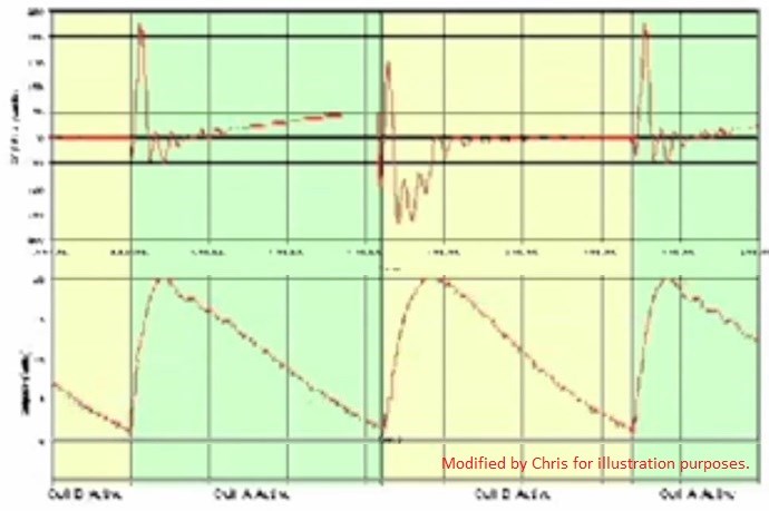
Here the scope shots from testing the frequency range, it reaches from 50hz to 170khz now , with infinite resolution, the upper limit is due to the external RC clock of the MC, using a dedicated external clock it could be extended further,also by reprogramming the PWMclock. at a cost of loosing some phaseshift resolution. Anyway the typical usage will likely be well below this frequency, as most switches become inefficient rising above this values. 

The puls duration can be adjusted from 500ns to 5ms independent from the frequency, or in complementary output mode as two signals 180 degrees out of phase, all with infinite analogue resolution. I will make a users guide with detailed information and a tutorial video explicating all the functions available.
Vidura
- Liked by
-
-
-

-
- and 1 others
Hey Vidura,
This is a perfect signal for the H-Bridge arrangement for the Input Switching.
The Difference between two Signals can give you what you need.
How many PWM Pins do you have?
Chris
- Liked by
-
Hey Chris,
I'm just uploading a video which should explain the basic features, it should be viewable in a few minutes.
The MC has the two phase PWM peripherical with analogous dutycycle which has two outputs, then there is a common single channel CCP digital PWM, which is unimplemented for the moment, but it can be programmed for a third channel, as it has the same system clock, it could be sincronized. For more channels- phases there can be connected additional MC's as they can be configured as Master and Slave devices via sync. connector.
Vidura
- Liked by
-
-
Hello all, here a first video explaining some features of the PWM module:
- Liked by
-
-
-
-
- and 4 others

The interactive and interchangeable modules is a very good idea.
great job vidura
Jagau
- Liked by
-
-
-
-
The latest progress, first assembly of a H bridge setup, to test the modules under load:


I had some minor issues still with the program code, when I activated deadtime in analogue complementary mode the processor
stopped some times, for the instance I left only the counter mode for the complementary output , which permits a 5 bit resolution for the shifting of duty cycles, which is ok for most drive requirements. The liberated dipswitch is now used to switch over one potentiometer for deadtime adjustments from 5 to 155ns. Anyway the independent mode is available with all full analogous adjustments for special applications.
Vidura
- Liked by
-
-
-
-
- and 1 others
Just to give you a idea of how fast PCB Way is i ordered a test circuit board on 5/30, i just received a shipping manifest stating i will receive my order on 6/04 from DHL. i can not even get that kind of service here in the USA not even Osh Park.
also i had a dollar off coupon so the boards only cost me 4 dollars plus shipping @ 10 boards <100mm x <100mm and this my friends is one hell of a deal.
this is of course for the electronic version of part G.
Keep up the good work.
Regards,
Marathonman
- Liked by
-
-
-
-
Hey MM I have no doubt about the service of PCBway, the problem here in Argentina is the local imposed puppets government, they work so hard to promote poverty and please the international monetary entities. The delays of delivery are not understandable, horrendous customs fees and inefficient clearance administration do the rest. Next month I'll traveling to Europe, there are better conditions for importing, so I thought to receive the materials there. Regards Vidura.
- Liked by
-
-
-
-
Hi all, Just some lines to keep you updated. For the moment I'm working on the production files for the first three modules PCB's,
I want to get out most possibilities from the hardware, taking in account some possible extensions or variations. I'm also evaluating possibilities to get the PCB's faster, this week I will get some estimates from local suppliers, I dont think to find a price nearly as cheap as PCB way, but if there is interest for orders in short terms it would be possible to resolve this way. Also I began to make the Slave Device , a second PWM module which runs synchronized with the main board, I had in mind some test setup's to experiment with the delayed conduction POC, testing timing in <us range. I still did not have the time to perform it, due to many difficulties in daily live, lately. I want to say Thank you to all supporting this work , and the Forum in general. Thank you so much! Ill keep you updated on the progress, more to come soon.
VIDURA.
- Liked by
-
-
-
-
- and 2 others
Here a short test of the first attempt of the PWM slave module, there is still a lot of work and solving issues ahead, anyway the resolution for timing between the boards is fine. The basic Idea is to use two phases of one board to drive a half- or H-bridge for the input and the second board for POC switching, eventually by a synchronous rectifier. Note that also a single main PWM board can be used for a single switch input and output with the same resolution between the two phases and that the dutycycle resolution remains constant when changing the frequency.
Vidura
- Liked by
-
-
-
-
- and 3 others
Hey Vidura,
Awesome work!
If we were to take The MEG as an example, we have a very straight forward waveform to replicate, known to work, verified by several other researchers. The correct waveform:
I was going to do a whole new thread on this ( Basic Facts as a Guide ) but I think you already have all that down! The input, two Short, perhaps 10% Duty Cycle Pulses. The Output Coils are bought into magnetic Resonance, where One Output Coil is Tricked into assisting the Input, and this is after the TVS Conduction, delayed Conduction. Normally of a very short duration, in the region you are adjusting for!
Vidura, I am so impressed! This is exactly what we needed! As a Community! Someone with the Electronics skills to bring a tool to the table with the flexibility to give the timing required. With only a little work, your Circuit will be able to produce the required signals to bring about Magnetic Resonance:
- Input Magnetomotive Force in the Positive Direction.
- Output Magnetomotive Force in the Negative Direction.
- Output Magnetomotive Force in the Positive Direction.
We trick one Coil into Assisting the Input Magnetomotive Force with the use of Delayed Conduction. Which is: 1 + -1 + 1 = 1.
Excellent Work Vidura!
Chris
- Liked by
-
-
-
-
- and 1 others
Hi All ,
some news here, when i got the estimate from a local PCB supplier for ten kits(60 boards ) was about 550$ !! in PCB way it's 50$ shipping included. I had already placed the order, still not payed, butI was not at all satisfied with the synchronization of the slave board, as the main PWM board with the external RC oscillator outputs a clock signal divided /4(system clock) for the slave board. So in the upper frequency range the slave board duty cycle was truncated as its clock was 4 times slower. So I looked for a suitable dedicated external oscillator, to feed the same clock frequency to both MC's. I wanted a simple reliable circuit with at least the same range then the actual version. In a application note for CMOS Schmitt-trigger I found a simple ring oscillator which performed quite good, including more extended range, only I have to get logarithmic potentiometers for the adjustment, as with the linear ones a sensible adjustment in the upper freq.range is difficult. So I cancelled the order, to upload the latest version when finished.
VIDURA.
- Liked by
-
-
-
-
I knew you would same a heck of a lot of money with them but 500 bucks WOW that is a lot of savings.
can you not find a duel output oscillator that outputs complementary and in phase outputs. or would this be the wrong application.
Marathonman
- Liked by
-
-
-
Yes you are right, the oscillator is used as a common time base for various MC's . As it is a signal im most cases it can be connected in parallel without inconvenience if wiring and conductors are chosen accordingly. There is a design in the Figurea thread where various decade counters are connected to a common clock source that way for a solid state circuit.
Vidura
- Liked by
-
-
-
Hi all!
Today finally I concluded the production files for the Tool modules , and thanks' to the support received from donations could place order for the first batch of PCB's. I also could include the slave module and some additional Power switch boards, so more complete toolsets will be offered. Here I will post the updated schematics and layouts of the modules.
Regarding the dedicated oscillator this is the basic circuit:

when testing I found that R2 had virtually no influence on the frequency, only distorted the signal a little at high frequencies, so I modified the circuit , the result you can see in the schematic of the 2phasePWM-v1.1 It was possible to extend the range from 23hz up to 360khz, the adjustment at the highest range becomes a little less sensible, but this should improve with the implementation of log potentiometers.


The designs can be used for non commercial implementation.
Regards Vidura.
- Liked by
-
-
-
-
- and 1 others
Hi all, The PCBs are ready, yesterday they have been sent for shipping. I will receive them in Europe next month, to avoid inconvenience with customs, as I have explained earlier. Meanwhile testing is going on, according the time I can invest at the moment. I still found a couple of Improvements to make, in first place the driver power supply is causing some interference in certain ranges, I will try to fix it adding filters , or otherwise change to a sinewave signal or DC output. The second issue were the connecting wires, it might be necessary to use shielded RF wires, as there are also some interferences in the signal when switching hard. Hopefully I will post some tests soon, also in other threads according to the topics, and to add some relevant information. Regards Vidura
- Liked by
-
-
-
Hi Vidura
Maybe you will have to use filters to reduce electromagnetic interference like these

in order to reduce the negative EMI / RFI effects?
Jagau
- Liked by
-
-
-
Hey Jagau,
yes this could work, i'll give it a try, as it is simple to add . The flyback transformer with short duty cycle is a bit noisy , maybe placing this kind of filter on the output of the supply will solve it without modification of the circuit.
- Liked by
-
-
-
yes vidura
Some time ago I was looking for a solution and this page had given me a helping hand
https://palomar-engineers.com/rfi-kits/am-broadcast-rfi-kits/
There is even a small calculation to know how often we want to eliminate
Jagau
- Liked by
-
-
-


No one online at the moment
In physics, scalars are physical quantities that are unaffected by changes to a vector space basis. Scalars are often accompanied by units of measurement, as in "10 cm". Examples of scalar quantities are mass, distance, charge, volume, time, speed, and the magnitude of physical vectors in general.
You need to forget the Non-Sense that some spout with out knowing the actual Definition of the word Scalar! Some people talk absolute Bull Sh*t!
The pressure P in the formula P = pgh, pgh is a scalar that tells you the amount of this squashing force per unit area in a fluid.
A Scalar, having both direction and magnitude, can be anything! The Magnetic Field, a Charge moving, yet some Numb Nuts think it means Magic Science!
Hello my children. This is Yahweh, the one true Lord. You have found creation's secret. Now share it peacefully with the world.
Ref: Message from God written inside the Human Genome
God be in my head, and in my thinking.
God be in my eyes, and in my looking.
God be in my mouth, and in my speaking.
Oh, God be in my heart, and in my understanding.
More than anything else, your contributions to this forum are most important! We are trying to actively get all visitors involved, but we do only have a few main contributors, which are very much appreciated! If you would like to see more pages with more detailed experiments and answers, perhaps a contribution of another type maybe possible:
They REFUSE to tell me why!
The content I am sharing is not only unique, but is changing the world as we know it! Please Support Us!
Thank You So Much!
-
Chris
110
-
 FringeIdeas
22
FringeIdeas
22

Ere many generations pass, our machinery will be driven by a power obtainable at any point of the universe. This idea is not novel. Men have been led to it long ago by instinct or reason. It has been expressed in many ways, and in many places, in the history of old and new. We find it in the delightful myth of Antheus, who drives power from the earth; we find it among the subtle speculations of one of your splendid mathematicians, and in many hints and statements of thinkers of the present time. Throughout space there is energy. Is this energy static or kinetic? If static, our hopes are in vain; if kinetic - and this we know it is for certain - then it is a mere question of time when men will succeed in attaching their machinery to the very wheelwork of nature.
Experiments With Alternate Currents Of High Potential And High Frequency (February 1892).
