Switching Tool Users Guide

  • Topic Is Locked
  • 1.8K Views
  • Last Post 30 December 2020
Vidura posted this 29 August 2019

This Thread is intended as users guide for the Modular Switching Tool. Also basics on switching and considerations for practical implementations in experiments will be covered in the thread. As first orders for the Switching Tool have been placed I beginn to release the users guide , although it is still not finished. If somebody whish to order  a Toolset or some Modules please contact me by PM, for the moment I will not publish in Ebay for the uncertain economic situation in our country. The thread will be locked in order to keep it as clear and short as possible. If there are any questions , or suggestions for editing they can be posted in:

Developing a modular switching tool

I will be happy to answer and add contents if required.

Vidura

Order By: Standard | Newest | Votes
Vidura posted this 29 August 2019

Introduction:
The Modular switching tool is a very practical commutation device for research on electromagnetics. It's features make it especially useful for pulsing DC applications, Half bridge and H bridge configurations, floating Hi or low side switches, coil shorting and other similar techniques.
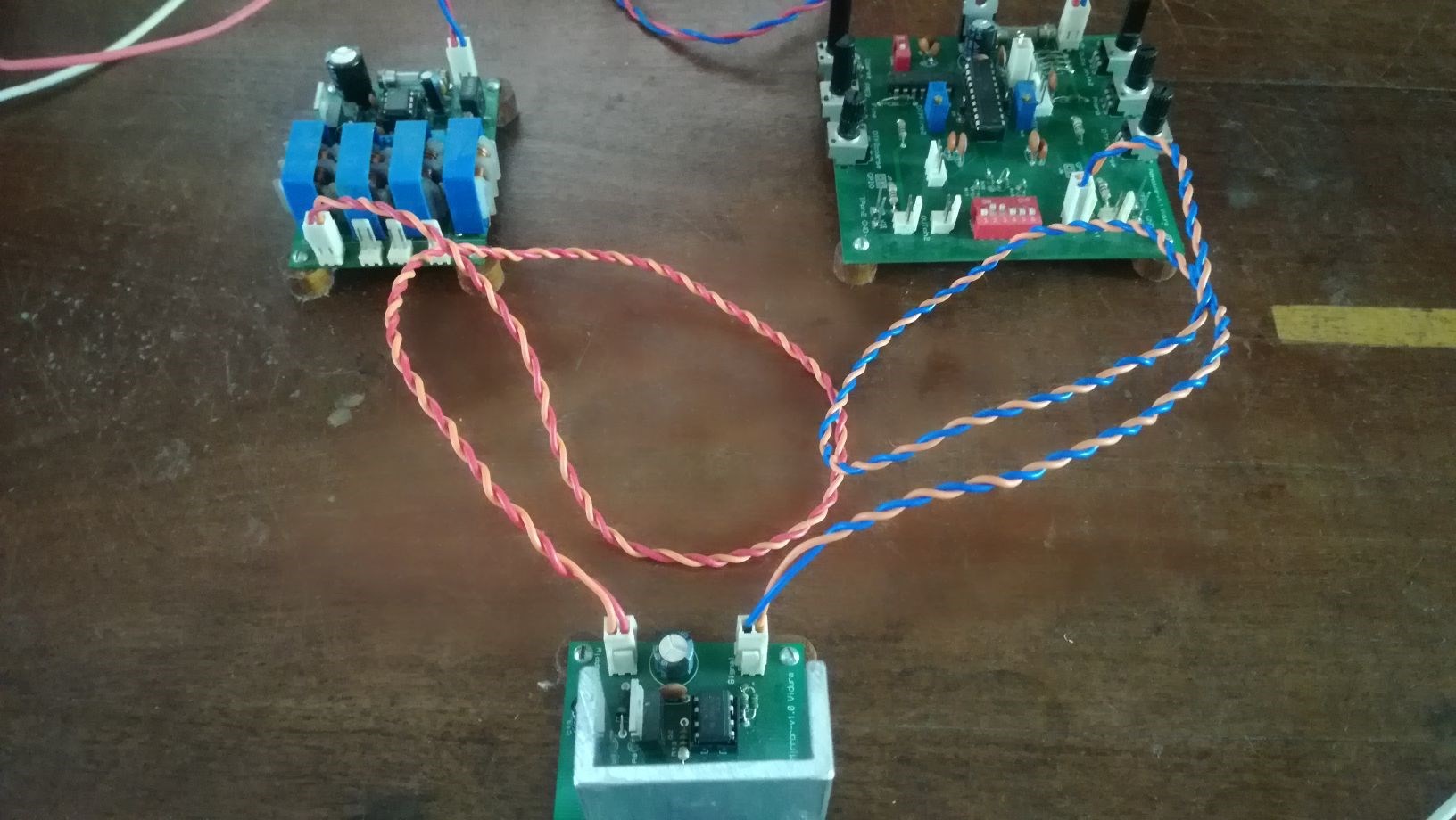
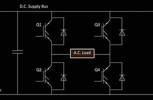
The power switch modules are provided with a single IGBT rated for 25A 1200V max. , which can be easily exchanged for a MOSFET Device, convenient for high frequency applications, by using the practical screw connectors. Additional screw connectors are provided for a surge protector, and connections to the external circuits. As the module employs an optical isolated driver, and the driver power supply is also galvanically isolated by transformers , the switch can be used completely floating, either in High or Low side position , combined with aditional switch modules as half or full bridge topology and more.
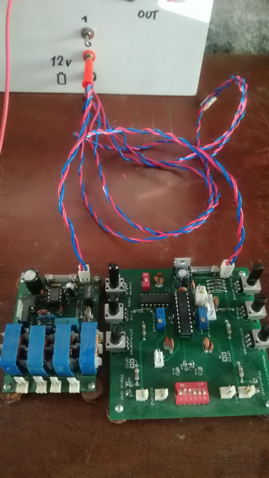
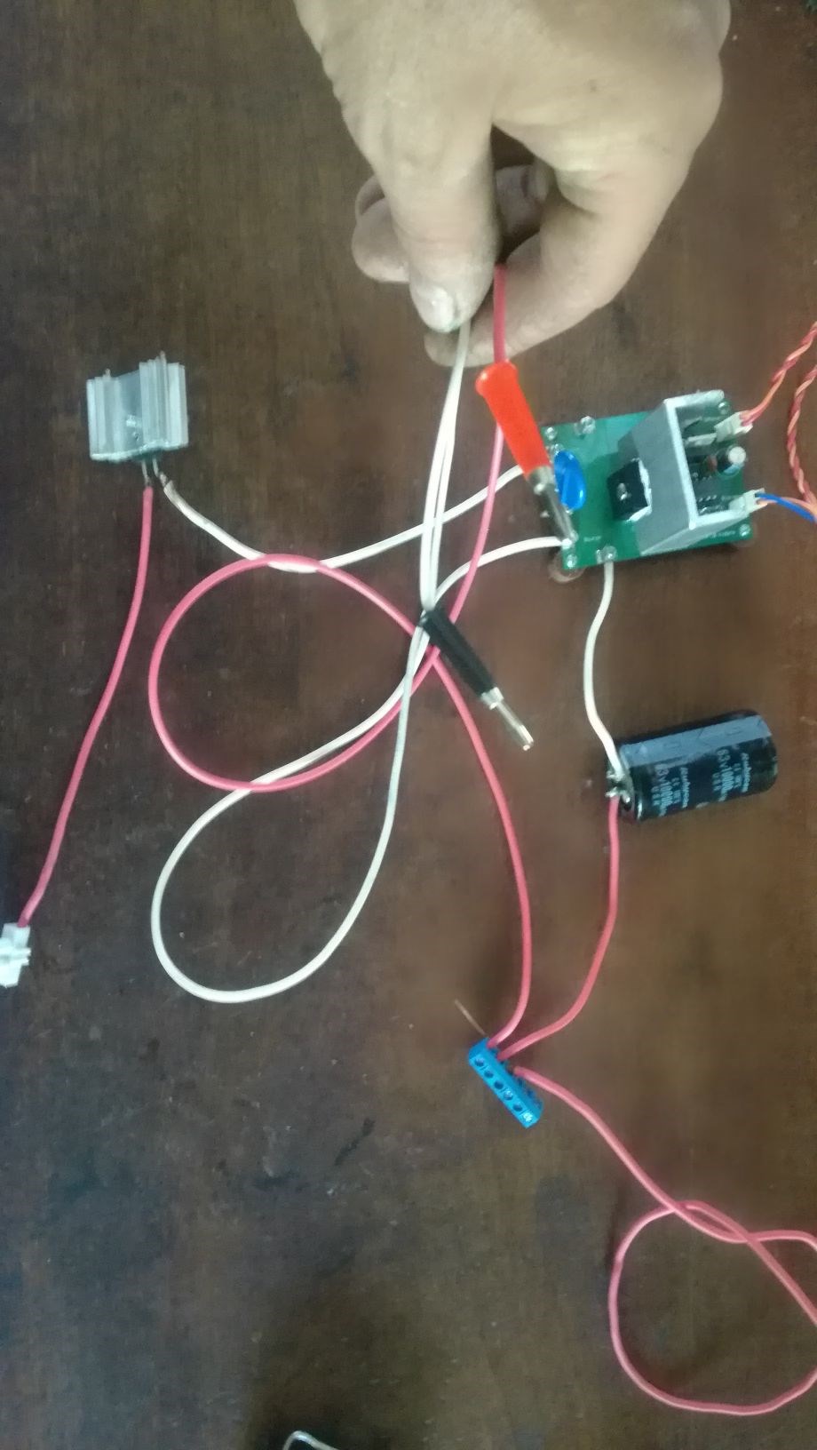
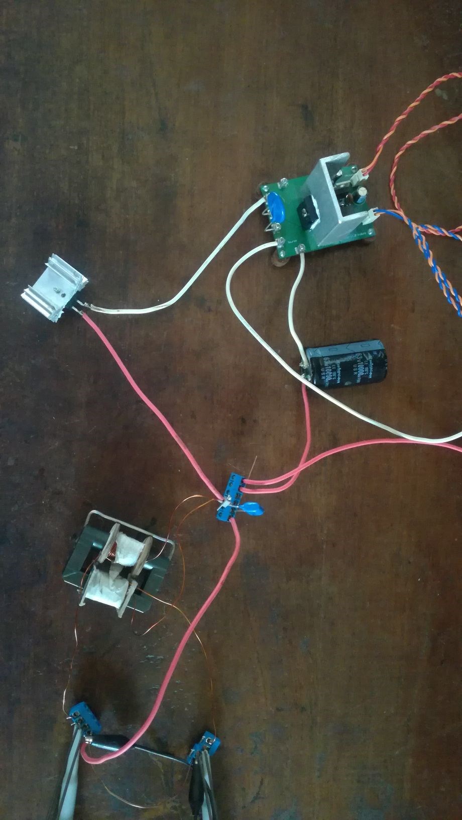
The Driver power supply module is another part of the tool, which provides four outputs to feed the required power for the drivers of four power switch modules. This device has to be powered with 12-15v dc, like a small lead-acid battery or a PSU.
With this two basic module types the tool can be used feeding the signals from a standard signal generator or an Arduino board. A set of connectors is available for this kind of usage.

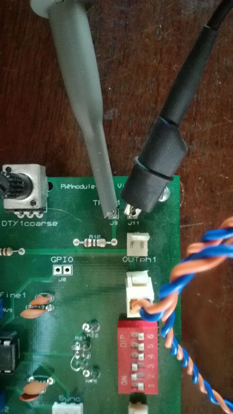
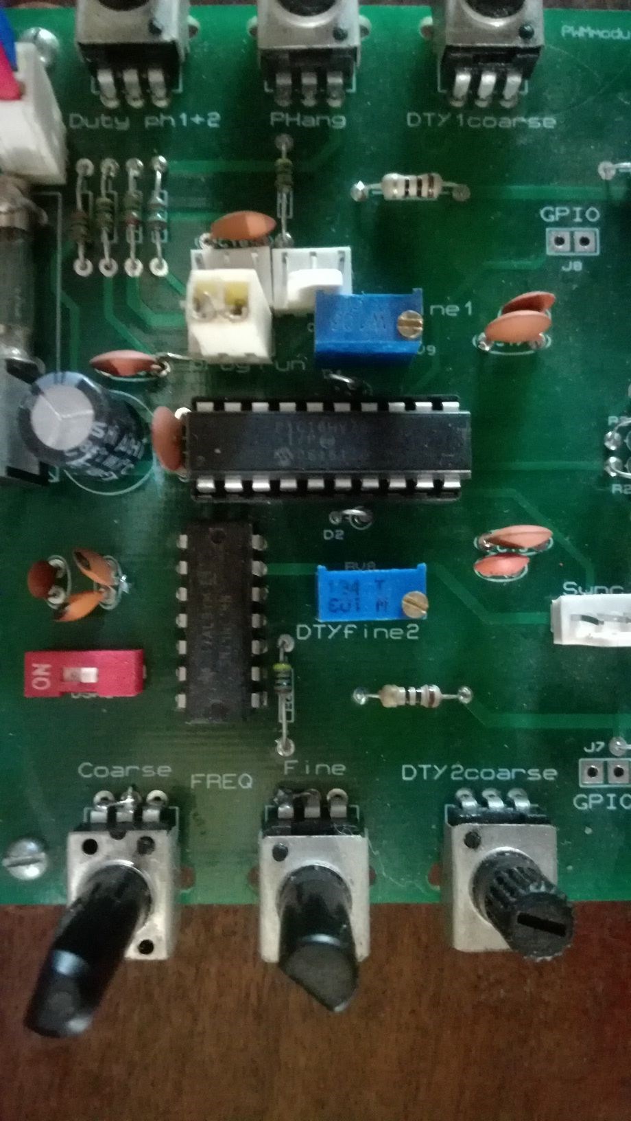
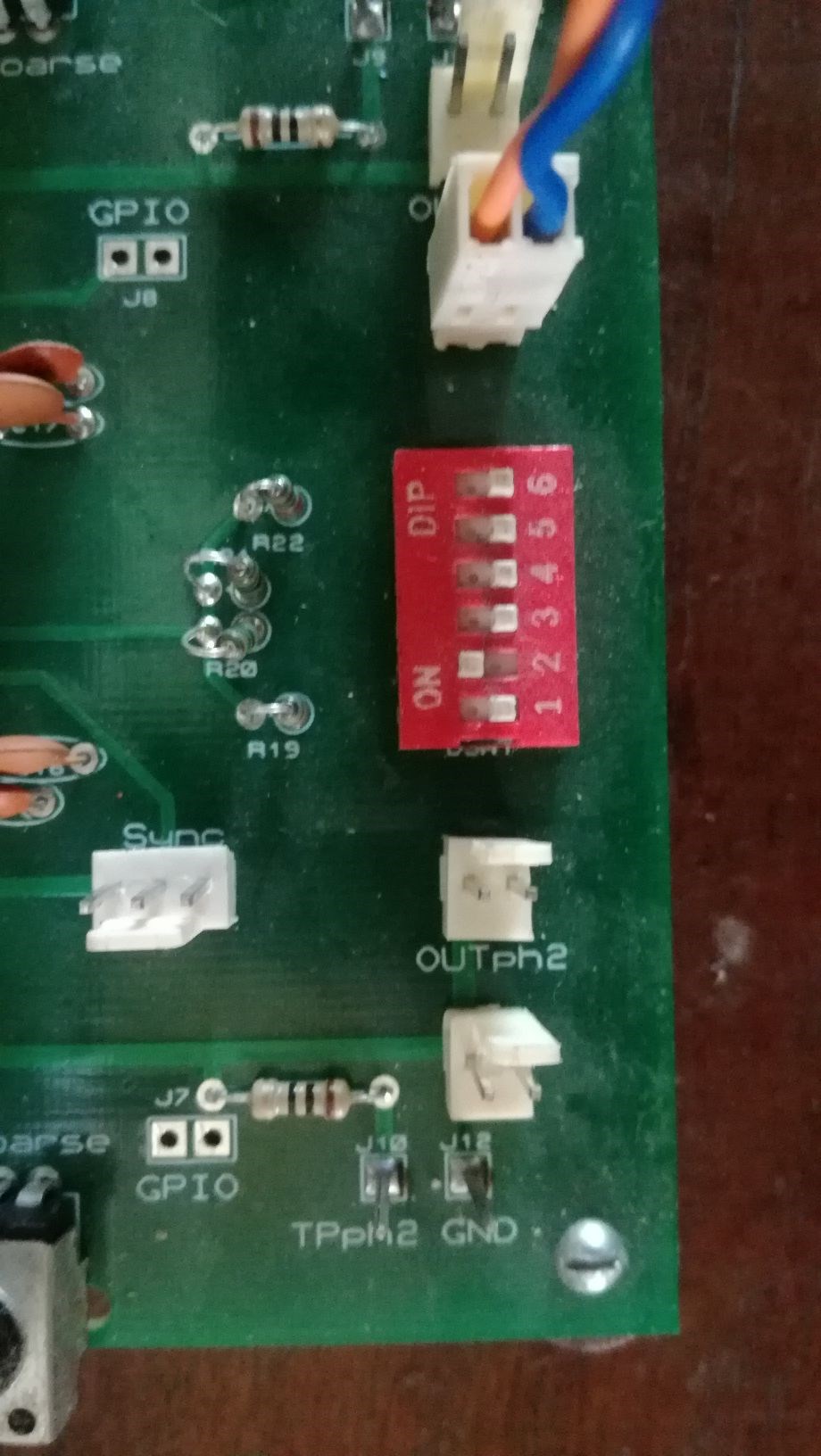
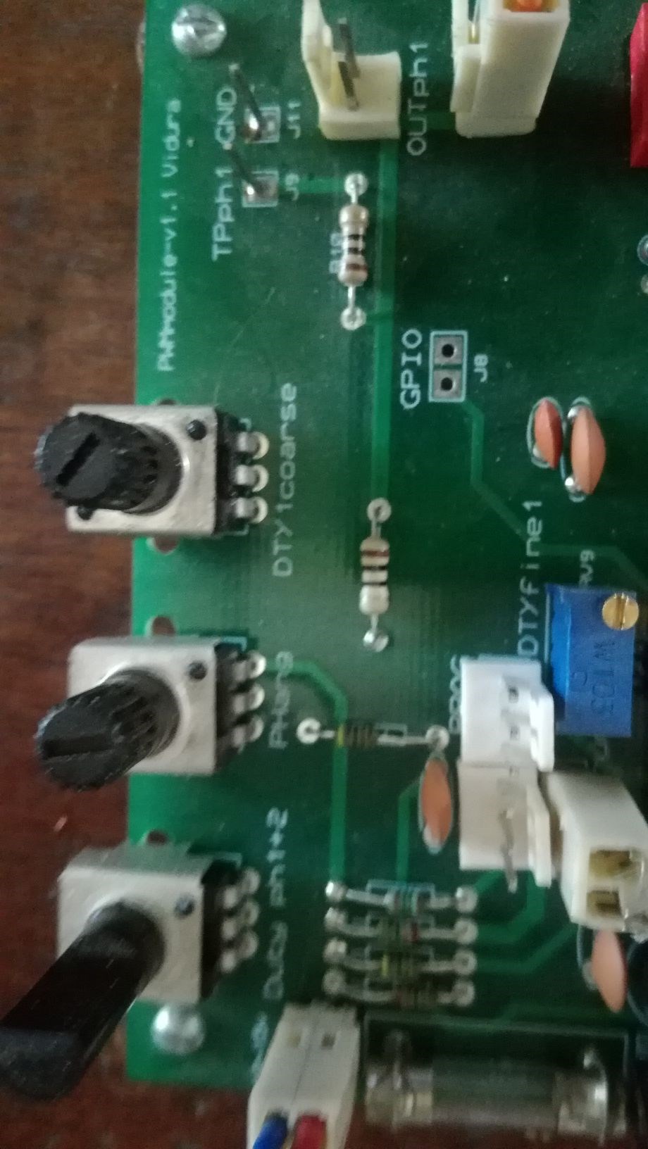
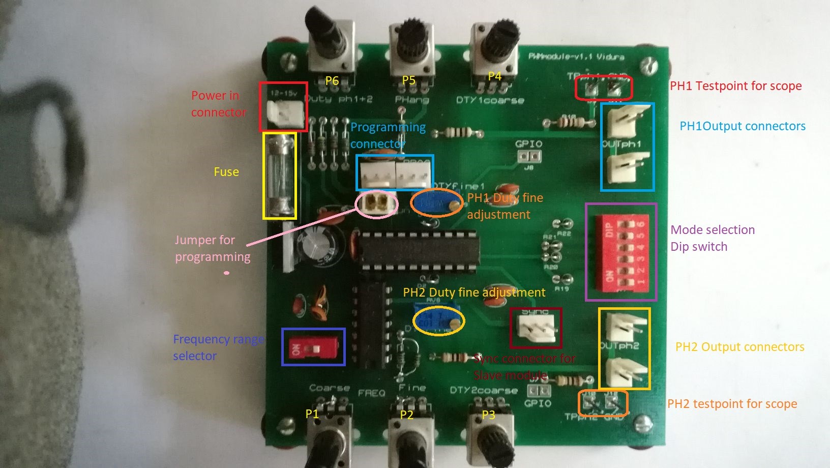
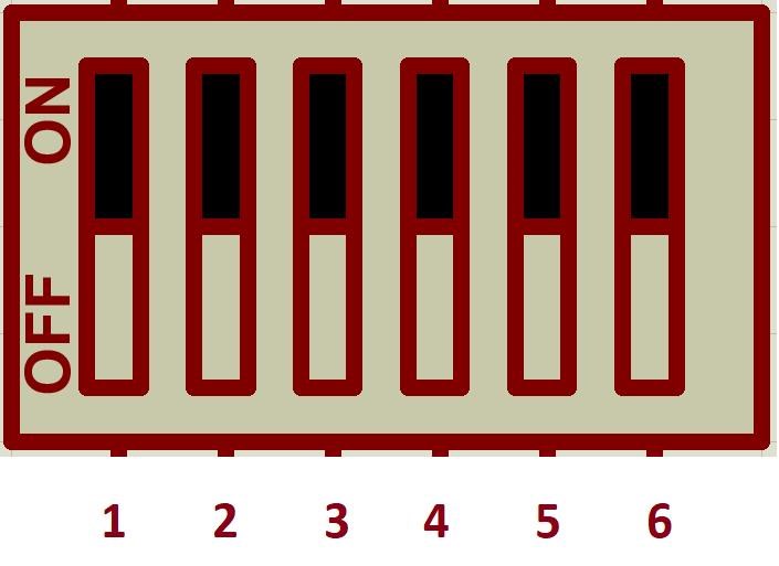
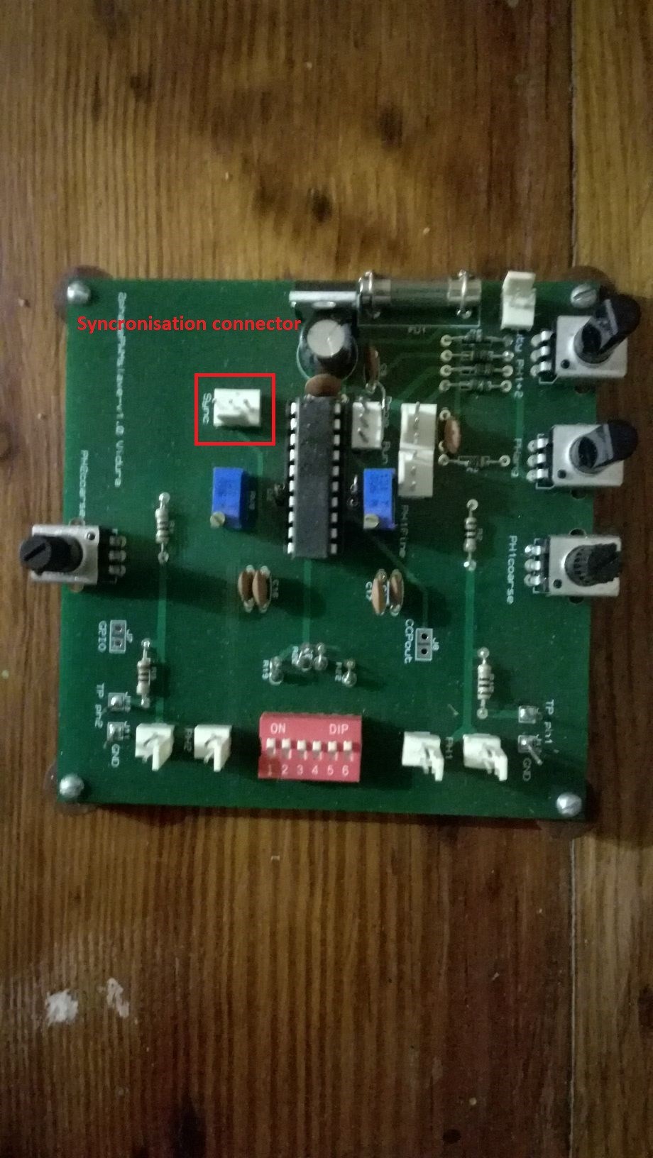
The next component is the Master PWM module. This is a specially designed oscillator which provides two phases of square wave signals, and have some unusual properties as the combined analogous and digital control feature. It is based on a PIC16hv785 microcontroller, this MC has a internal two phase PWM peripherical with infinite resolution analogous duty cycle control. Also the frequency of the PWM is analogous adjustable , and thus have infinite resolution as well. This advantages are combined with digitally controlled features like the 5 bit resolution of the Phase angle, complementary outputs for half or full bridge drive with adjustable deadtime, or individually adjustable duty cycles for both phases. The device have various ranges of frequencies and duty cycles , and covers a spectrum from a few Herz up to 350khz. Also a connector for in circuit programming is on the module, for those with knowledge in PIC programming more possibilities like an additional CCP peripherical, OpAmp's and timers and a synchronisation feature for a slave module, for adding two more phases, are available in the MC.

The slave PWM module:
This is a module which is intended as an extension, it adds two more phases synchronized with the master PWM,
It is basically identical with the master PWM, with the only difference that it do not have an own clock oscillator, as it is designed to be connected and synchronised to the master PWM module via a sync connector.

Hardware overview:

1.Power switch module:

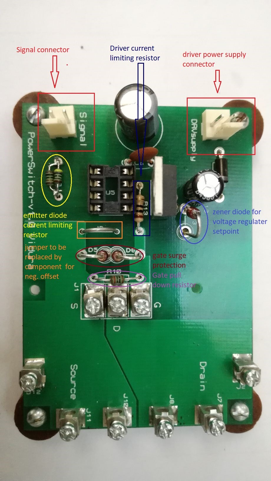
This is a view of the Power switch PCB with identifiers for some components with specific functions.
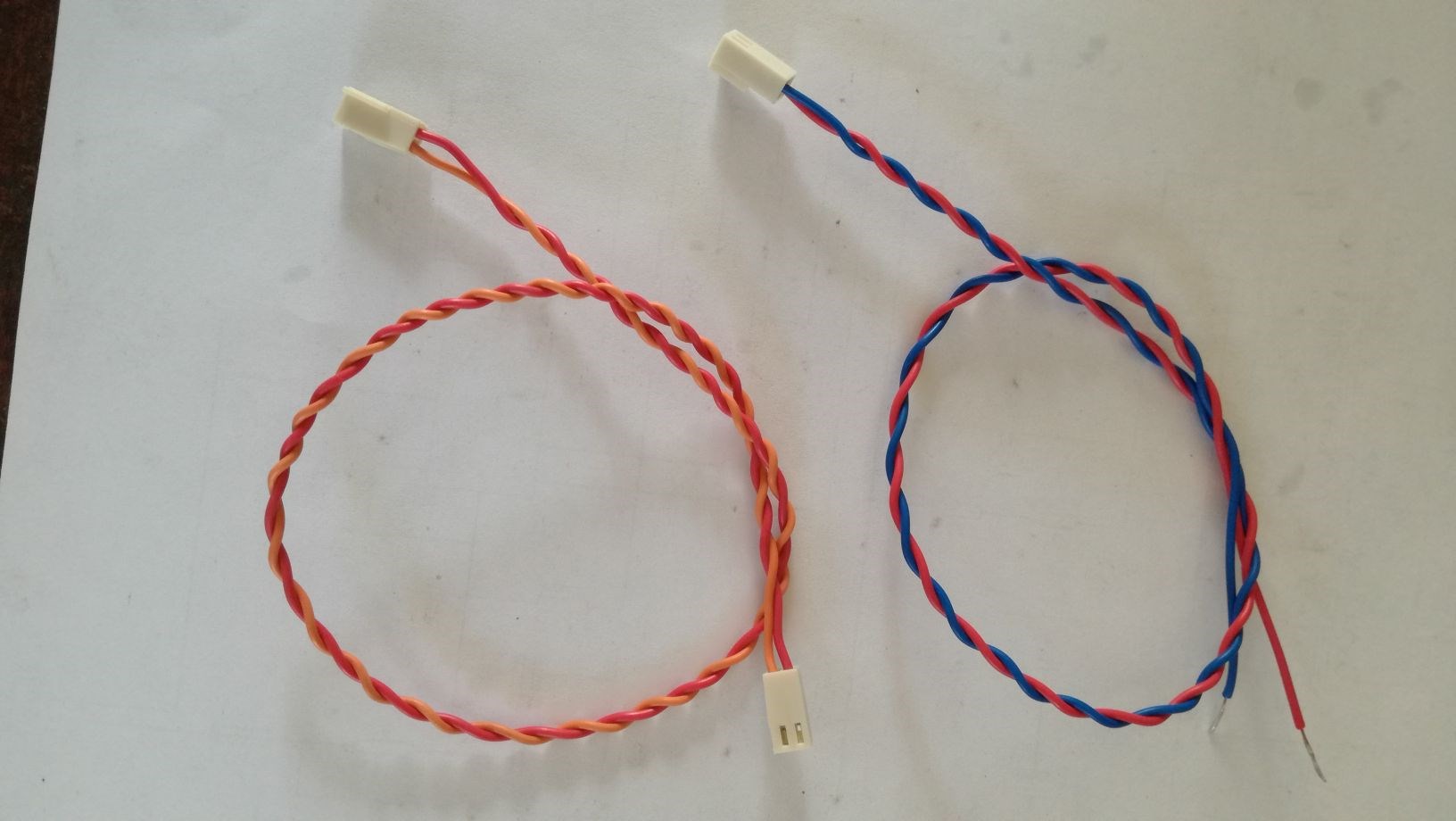
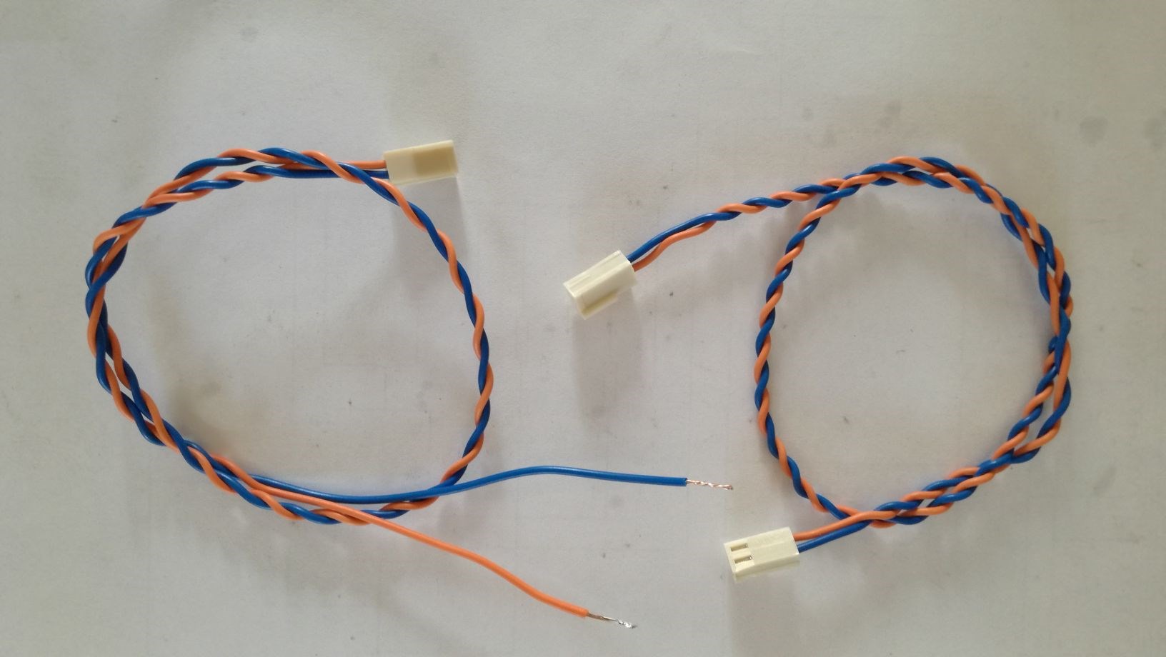
Signal connector: to connect the signal source, which can be the PWM module, a signal generator or similar. The positive terminal is on the right side in this view, the slot side of the connector. The Signal connector wires have Orange-blue colour identification. (orange corresponding to the positive conductor)
Below it remarked in yellow the current limiting resistor for the emitter diode of the driver IC. It is configurated for a voltage of 5V, as output from the PWM modules. Using a signal generator it should be set to the same voltage, although for some models it might be necessary to rise it to 10-12 volt, you can put a 1 ohm resistor in the signal line and measure with the scope , to find the correct voltage setting for your SG. Be careful not to exceed 16mA, as the driver IC could be damaged by doing so. For some Arduino boards with 3.3V output the value of the limiting resistor should be changed to 180- 220ohm to achieve a reliable switching performance.
On the upper right side you find the Driver supply connector. Here the connector wire from the Driver power supply have to be placed. The corresponding connection wires are identified with red-orange colours. The Driver power supply delivers AC current at aprox.40V which is rectified and filtered in the Power switch module.
Below remarked in blue you see the zener diode for the voltage regulator, it defines the setpoint for the voltage limit for the driver IC. It is by default set to 17V (18V zener diode -1 voltage drop). The A3120 driver IC is capable to driving voltage up to 30 V, which is within the range of many IGBTs, But most MOSFETs have a max. Gate voltage of 18-20V, so the default regulation can be used for both types of switches. In the centre you see the deriver current limiting resistor, it has two functions, it prevents ringing on the gate and limits the maximum current drawn from the driver IC . The default value of 10 ohm should cover well most applications.
The Jumper remarked in orange colour is a special feature of the module, It can be replaced by Zener diode to achieve a negative offset switching, this special technique will be covered later in another chapter.
Remarked in red the gate surge protection, consisting of the two zener diodes D5,D6. Their function is limiting the gate voltage below 19V. This maximum value is adequate for MOSFETs, and although some IGBT can be driven with higher gate voltage, for most applications they will perform good with the default values.
Below it marked in violet you can see the gate pull down resistor, its function is to keep the switch in off state, for example when the driver supply power is turned off.

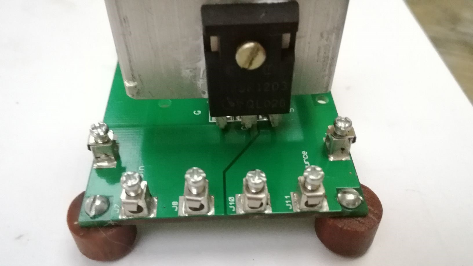
In this picture you can see the IGBT mounted in the module. Care must been taken to connect the gate to the corresponding terminal labelled with G. In your toolset you might have normal and mirrored versions of the switch module, the mirrored version have the IGBT on the opposite side of the heatsink, and the leads are bent to the opposite side to match the correct connectors. If you change the switch device assure to mount it in the correct position for each type of module. IGBTs and MOSFETs in TO247 or TO220 packing have the gate always on the left side looking at the front of the device.

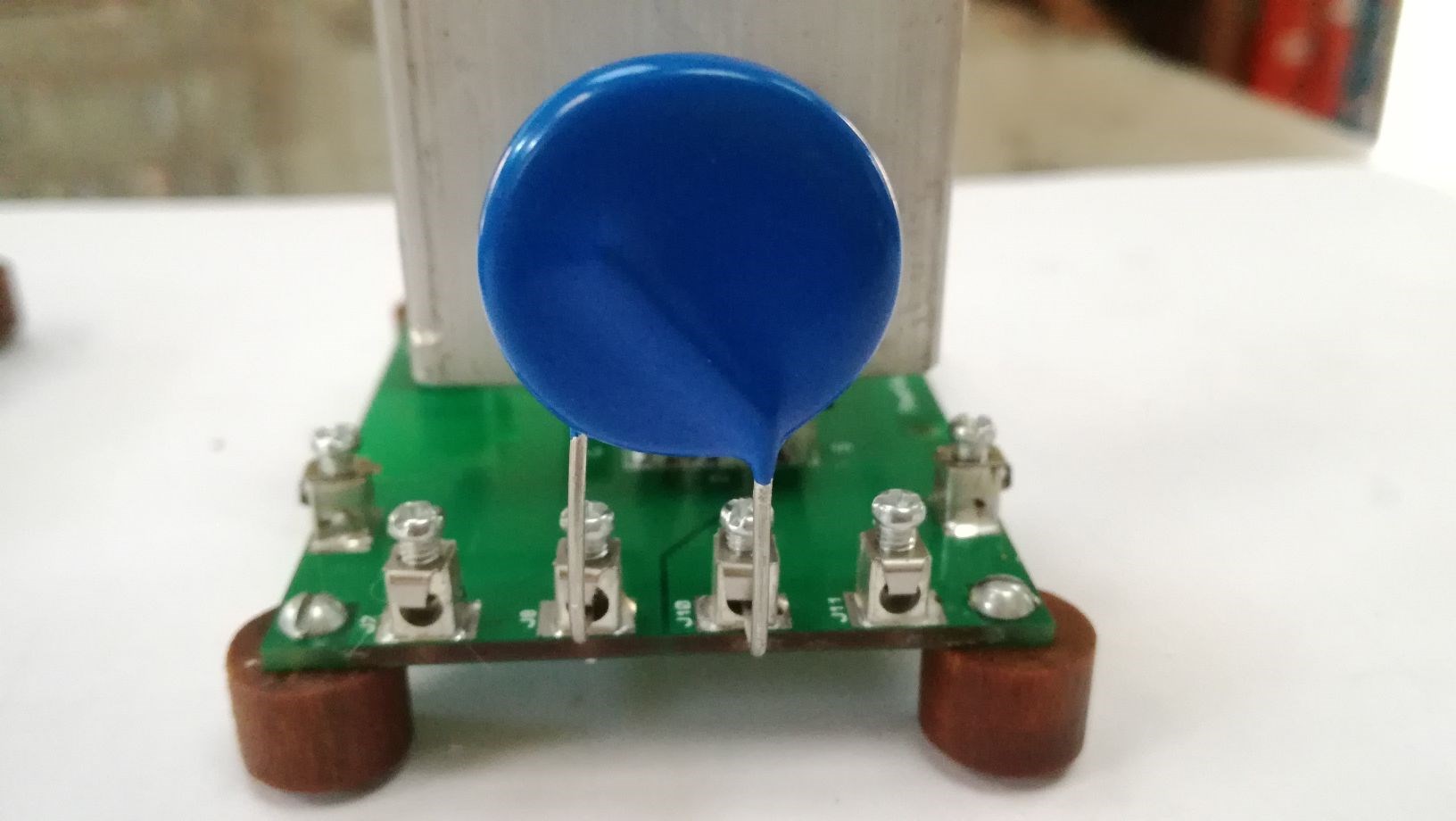
The Drain-Source surge protector. This is a very important part when you are switching inductors, as the BEMF spike would easily destroy the switch if not present. The default component is a MOV S14K275 witch has a max clamping voltage of 710V, this leaves a good safety margin to protect the IGBT (1200V max), but if needed it can be exchanged for a higher value up to a 420V rms MOV which clamps at 1120 Volts. If you change the switch look in the datasheet for the rated maximum voltage and use an appropriated surge protector for the new component. For lower voltage devices also a TVS diode can be used.

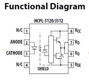
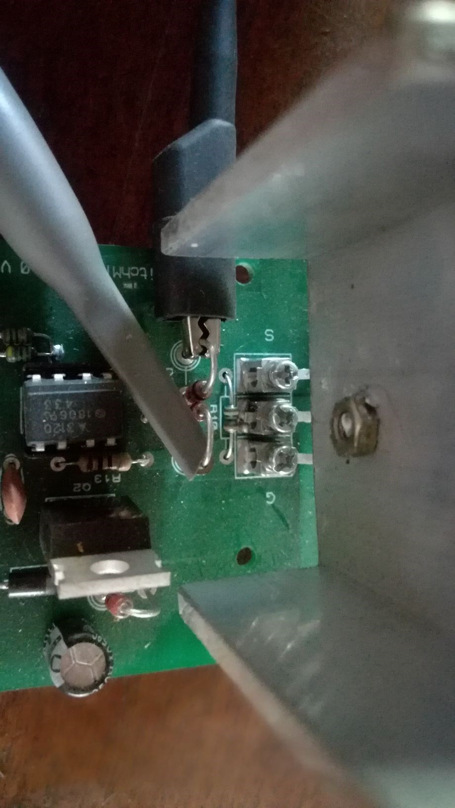
The optical isolated driver:

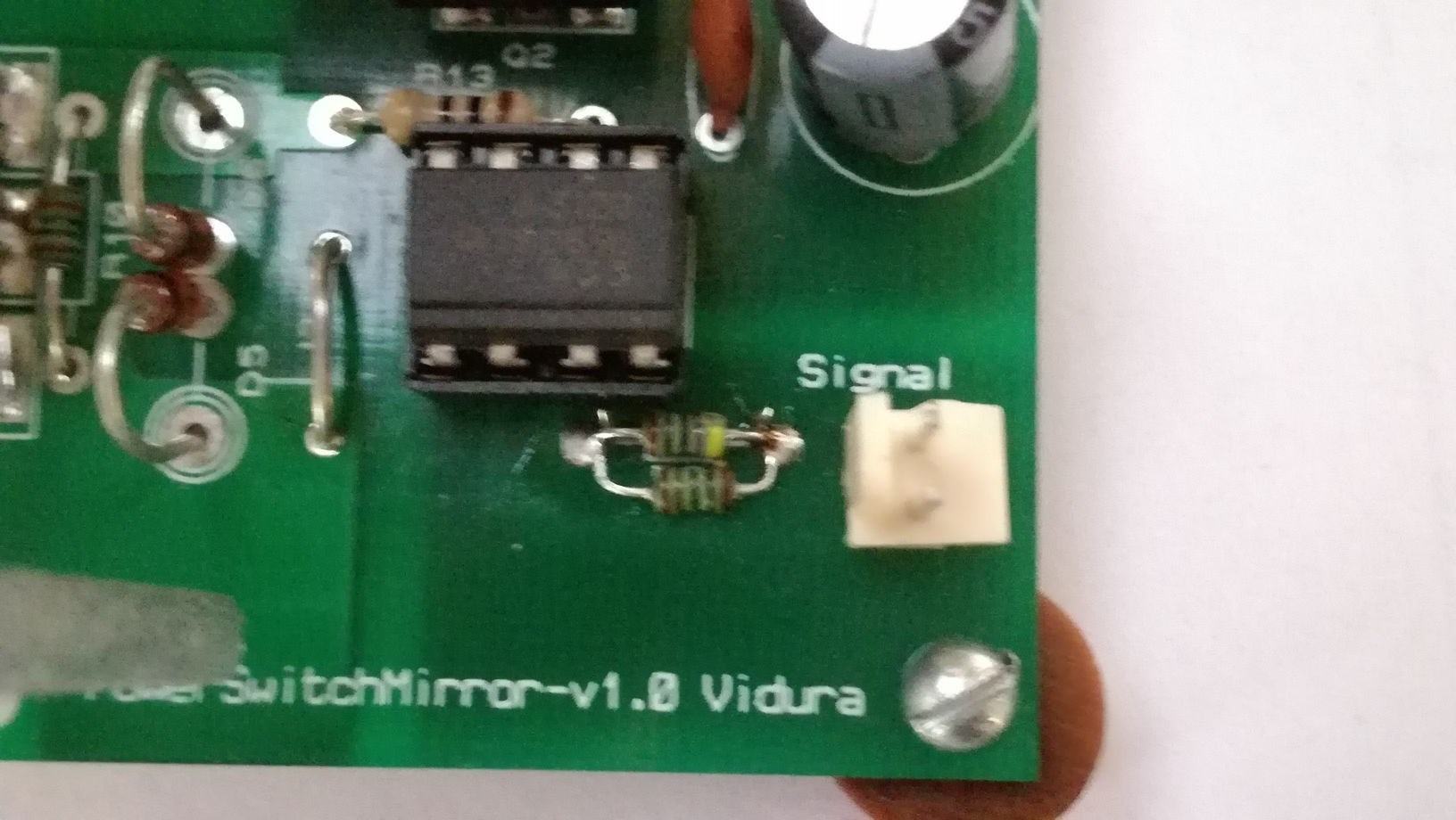
In this image you can see the optical isolated driver IC, if you remove it in any occasion be sure to mount it in the correct position like shown , the identifier stripe is always on the signal input side. If any signal source with a different voltage as 5V default configuration will be used , changing the current limiting resistor of the emitter diode may be required. Choose an adequate value to adjust the emitter current between 10 and 16 mA.
Below a functional diagram of the driver IC:

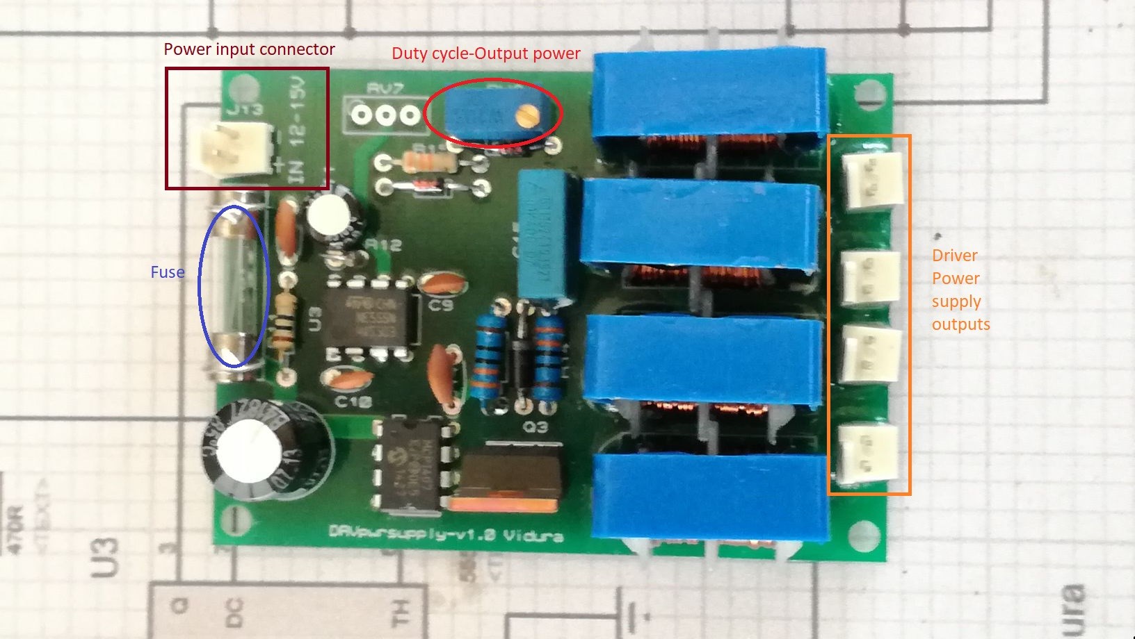
 2. The Driver Power supply:
The module is designed as a floating power source for the Driver IC on the Power switch modules. The four separate output transformers covered with a dielectric coating are providing an galvanically isolation up to 4000Vrms. In the image below you can find the indicators for the connectors and the output power adjustment.
The module has to be connected to a 12-15Vdc supply, which can be a 12V lead-acid battery or a small PSU.
With the default regulation four modules mounted with MOSFETs of moderated total gate charge can been driven up to more than 200khz, rising the input of the supply module to 15v it supports even higher frequencies, the same applies if less modules are connected. If more driving power is required the duty cycle can be increased, by turning the preset potentiometer clockwise. 

Vidura posted this 11 September 2019

Getting Started:

1.Power supply:
The Driver Power supply module, the PWM master module and the PWM slave module have to be connected to a DC power supply with 12 -15V output. Any 12v lead acid battery is well suited , or a small PSU with 12-15 V and
1 A min output. Check the polarity and use clear identification, as the modules are NOT REVERSAL CONECTION PROTECTED.

2.Feeding a signal from a signal generator into the Power Switch Modules:
This modules are calibrated for a signal 5Vpp , so when they are connected to the PWM modules or any 5V Microcontroller no adjustments are needed. If using the SG as signal source, testing has shown that a higher voltage has to be set to get the correct current for the signal entrance of the Power Switch Module.In the following video you can see how to calibrate the SG to the correct voltage setting before start using the modules:

Vidura posted this 28 October 2019

How to use the PWM module step by step:

Part 1 Free running mode.

First we have to connect a 12-15 V dc supply to the driver power supply and the PWM module.

Then we have to connect the red-orange connector and the blue-orange signal connector to the Switch module:

In the following example we use a single low side switch, so we have to connect to our power supply:

we connect the negative to the source of the mosfet and the DUT on the positive rail, an capacitor in parallel to the supply enhances the performance:

The blocking diode is optional, it depends on the setup if we should use it or not. It prevents the current to return yo the supply.


We can connect a scope probe to the test point of the corresponding channel, this way it will be isolated from the DUT.
or we can place it as follows to the mosfetgate, for monitoring the actual signal on the switch. Care has to be taken for not shorting to other points by scope ground loops!

Then we will select the frequency range with the DIP switches. We choose the high range, single DIP switch Off position(3-350 khz)

And on the configuration switch we set the short range for the pulstime(1+6 Off) and Free running mode(Sw2 ON)

the clock divider is set to 1:16 (4+5 Off)

Then we can adjust the pulsduration with the potenciometer PH1 Duty, and extend the duration with the potenciometer PH1+2 if needed. the frequency is adjusted with the coarse and fine potenciometers.

When using the free running mode we have to take care that the puls duration will be constant while changing the frequency, so when increasing the frequency, the duty cycle eventually can reach almost 100%. so it is a good practice to check the signal if in the expected range it stays in safe values, before powering the device, eventually adjustments have to be made. for sweeping thru wide frequency ranges with a percental duty cycle we can safely use the complementary output mode , this will be covered in the next chapter.

Vidura posted this 07 December 2019

Hi Friends.
Here I will present a special switching methode, called the negative offset switching, and will explain how it works in the following short video. Although you swill not need this for most applications, it can be very beneficious for some hi frequency applications, or some special cases where a very fast switching is required.

In the next post I will add the instructions and a schematic for the needed additional parts.

Vidura

Vidura posted this 01 September 2019

3. The PWM Master module:
This is the signal source, a two phase PWM module with combined analogue and digital features. It is based on an enhanced 8bit MC, the PIC16F785 with specific peripherals, as the dual phase PWM and two hi speed comparators, which are used for analogue duty cycle adjustment with infinite resolution. To overcome the limited period resolution typical of digital PWM devices, an adjustable external oscillator is used to clock the MC, which allow an infinite period resolution over a wide range of frequencies as well, in combination with the internal frequency pre-scaler. In the image below the most important parts are indicated :

-the power in connector: With the provided connector identified with red and blue wires a 8-15 volt supply has to
be connected(conveniently the same as for the driver power supply).

-Fuse: a 600ma fast fuse.

-Frequency range selector: this switch is used to select between two ranges of the oscillator. The low range covers
from 6Hz to ~3kHz, and the high range from ~2.5kHz to >300kHz for the PWM outputs.

-Mode selection Dip switch: Here various different modes of operation and adjustment ranges can be set as follows:


Switch 1 Duty cycle range Phase 2 off = low range on = hi range (used in free running mode only)

Switch 2 PWM mode selector off = free running mode on = complementary output mode

Switch 3 P5 adjustment mode off = P5 is used for deadtime adjustment (used in complementary output
mode only)
on = P5 is used for phase angle adjustment in free running mode and for
duty cycle adjustment in complementary output mode (5 bit resolution)
Switch 4 and Switch 5 set the internal clock prescaler for the PWM module as follows:
Switch 4 and 5 off = clock frequency divided by 8
Switch 4 on and Switch 5 off = clock frequency divided by 4
Switch 4 off and Switch 5 on = clock frequency divided by 2
Switch 4 and 5 on = clock frequency divided by 1 (highest range)
Switch 6 Duty cycle range Phase 1 off = low range on = hi range (used in free running mode only)


-PH1 and PH2 Duty cycle fine adjustment: This preset potentiometers are used to adjust the minimum duty cycle in free running mode, the minimal value is ~400ns . They can also been used for finetuning the duty cycle in the upper frequency range.

The potentiometers:
-P1 for the frequency broad adjustment
-P2 for frequency fine adjustment
-P3 Phase 2 duty cycle adjustment (used in free running mode only)
-P4 Phase 1 duty cycle adjustment (used in free running mode only)
-P5 has various functions:
If switch 3 is in off position and switch 2 in on position it is used to adjust the deadtime
in complementary output mode between 0 and 155ns.
Important note: in the upper frequency range >200khz the deadtime values above 75ns might not be
selectable. For running the PWM in complementary output mode up to the max. Frequency a small
value for the deadtime must be set previously. If operating in this frequency range, please check the
signal on the test points with the scope before running the Power switch modules.
If switch 2 and 3 are in on position (complementary output mode), P5 is used for duty cycle adjustment.
If switch 3 is in on and switch 2 is in off position (free running mode), P5 is used to adjust the phase angle
between the two phases.
-P6 is used for the duty cycle adjustment of both phases together (used in free running mode only)

-Beside the mode selection switch are the signal out connectors for each phase, with a test point and ground for
each channel for connection of the scope probes.
-the Sync connector provides the processor clock signal and a synchronisation pulse for a slave PWM module.
-Jumper for programming. For normal operation it has to be set to "run" position. For the in circuit programming
feature change to "prog" position.
-Programming connector: you should be familiar with PIC programming for using the in circuit programming
feature, a PIC programmer(as PICkit3 or 4, or ICD3 or 4 available from Microchip) can be connected to this
connector for changing the firmware settings, or add additional functions to the PWM module.
-More details will be covered in the introduction of practical implementations.

4. The PWM slave module:
This module is nearly identical to the PWM master module, only that there is no oscillator on this module and thus no frequency control potentiometers. It is connected to the PWM master module , which provides the system clock for the slave module, and a synchronization pulse to keep the PWM slave module phase locked to the PWM master module. Normally both PWM  modules should be set to the same frequency prescaler settings, But for some specific requirements with different settings some tricks can be achieved. More of this will be covered in the practical applications section.Here in this image only the connector for synchronisation is identified ,as all the other controles and components are identical to the PWM master board:


5.  The connectors: The Modular Tool Kit provides the connection wires for the modules identified as follows:

-The connectors identified with red -orange colour wires are used to connect the Power Switch Module with the
Driver Power Supply Module.
-The connectors identified with red-blue colour wires are used to connect the PWM modules and the Driver power
Supply to a 12-15V DC source. Red wire positive-blue wire negative.
-The signal connectors are identified with orange-blue colour wires, the terminals are mirrored to the power
connectors to avoid erroneous connections. The connectors with terminals on both sides are used to connect the
Power Switch Modules to the PWM Modules, and the connector with a single terminal is used to connect to the
signal generator or Arduino board.

This connector is for the synchronisation of the PWM master and slave boards, a screened wire is used to reduce interference.


Vidura posted this 15 September 2019

A brief Introduction on Switching:
If we want to use MOSFETs or IGBTs in our experiments or designs it is very important to realize that these semiconductor devices are designed as ON-OFF switches. Unlike Bipolar (power) transistors, which are capable to amplify in linear manner the signal current and thus output any potential or current within the range of the applied supply voltage. This means that MOSFETs and IGBTs are intended to deliver either a HI or a LOW output , and not any intermediate values like bipolar transistors, but they can do this switching very fast , depending somehow on the device. So why we use this kind switches, what is the advantage, what the drawbacks? We could ask if it would not be better to use bipolar transistors, as they can amplify different waveforms ,as triangle, sawtooth, sinewaves. And that is indeed true for some applications, like audio amplifiers for example, but they have the disadvantage of a poor efficiency, because delivering any power levels which are different from fully ON or OFF are leading to heat dissipated in the Transistor. And this is the main reason why in modern power electronics in almost every application MOSFETs and IGBTs are used. This devices have a very low resistance in the ON state, and turns virtually into a isolator when switched OFF. This makes them specially suitable to produce current pulses of different Frequencies and Duty Cycles (PWM) useful for many different kinds of engineering solutions.
With this techniques currents can be controlled very efficiently, and for example in Inverters or motor controllers Sinewave currents are sampled from pulses and can achieve efficiencies above 95% .

The Gate Driver:
For efficiently switching MOSFETs and IGBTs these have to change between ON and OFF state as fast as possible. As there is a zone in between this states, near the gate threshold voltage where they behave unstable, and resistance will increase and lead to heat losses, also oscillations due to coupling can occur in this condition. The gate of this devices have a capacitance, it is like a small capacitor which has to been charged and discharged in each cycle. For an efficiently switching the transition between ON and OFF state should be as fast as possible to reduce losses due to heat dissipation. For this purpose special IC have been developed: the gate driver IC. This devices basically amplify the incoming signal and charge and discharge the gate capacitance of the MOSFET or IGBT. The driver current rating is usually specified in Ampere and means the peak current which the IC can source or sink in an pulsing manner. In the Modular Switching Tool the A3120 Driver IC is used, which has the special feature of an integrated optoisolator, providing a galvanically insulation between the signal source and the switched circuit. This driver has a peak current of 3A and can handle a supply voltage up to 30V , which would be way too high for most MOSFETs, but some IGBTs can be driven by such high a high gate voltage. The default driver supply voltage of the Power Switch Modul is 17V which can be used for most MOSFETs safely. If you change the provided switch in the Power Switch Modul for another device, please check in the datasheet for the recommended gate voltage. If needed the driver supply voltage can be modified by changing the zener diodes on the Power switch Modul.

Vidura posted this 15 September 2019

LOW side, HIGH side and FLOATING switch:
First we will have a look at the most common and also most simple to employ configuration for N-MOSFETS or IGBTs. This is the LOW side switch. In this case the source or emitter is tied to the ground of the circuit, and the load connected to the Positive Rail and the drain or collector of the switch. If we have an inductive load the BEMF
Appearing on the drain or collector will be of positive sign. This configuration have the most simple driving requirements, as the gate driver IC and the signal source can have a common ground with the switching circuit.

The next configuration is the HIGH side switch. Here the drain or collector is connected to the positive rail, and the load to the source or emitter and to the ground of the circuit. If we have an inductive load connected, the BEMF on the source or emitter will be of negative sign. The HIGH side switch is much more complex regarding the driver requirements, because the source or emitter , which have to be connected to the driver IC is changing in potential when the switch turns on or off. When using a standard driver IC this would mean that it's ground connection and the signal ground has to be connected to a point with continuously changing potential of the circuit. So in this case special solutions or driver IC are needed. But fortunately the Switch Modules of the Tool Kit are already designed to operate in any configuration, so we don't have to worry about that.

There are two commonly used combinations of the above described configurations which produce a AC output:
The Half bridge combines one high side and one low side switch, this configuration needs a symmetrical power supply, which can be achieved for example like in this circuit :


The capacitors C1 and C2 provides the symmetrical power supply, and C3 is a so called DC blocking capacitor. It's function is to prevent unbalance of the potential between C1 and C2.
C3 have to be selected according to the operation frequency.
A drawback of this configuration is that only 1/2 of the rail voltage will be available on the output as AC.

The Full Bridge or H-Bridge:
In this configuration two high side and two low side switches are combined , or in the case of a three phase inverter we need three of each. In this case the full rail voltage is available as AC output, the basic circuit looks like this:


Both of the last configurations are mostly fed with complementary signals, which means that when one signal is high, the other is always low. If the signals are overlapping a shorting will occur and the switches could be damaged. The PWM modules of the Tool Kit provides a complementary output mode, where the relationship of the duty cycles can be adjusted in 32 steps, and an adjustment of the deadtime(when both channels are OFF) from 0 to 155ns. But it is also possible to feed pulses in independent free running PWM mode, where the duty cycle is adjustable independent from the frequency for each channel separately. If you choose to run a half or full bridge in this mode take care that the signals will overlap at some point when rising the frequency, so the signals should always be monitored or respectively the frequency limited in a way that no overlapping will occur.

The last configuration is the Floating Switch: In this configuration neither the drain-collector nor the source-emitter is connected to the positive or negative rail of the circuit, it can be connected "floating" on any potential in a circuit, for example in a coil shortening technique, where taps of windings in the middle of a coil are shortened-unshortened. Also in this special cases we have the advantage of the complete galvanically isolation of the Power Switch Modules, so we can simply put our modules in any required connection, without worrying about complex switching circuitries.

Vidura posted this 21 September 2019

Hello All,

In first place please apologize the delay for the promised tutorials for implementation of the switching tool. Due to time restrictions and some issues for editing videos with my phone I didn't get there still, but I promise to start a tutorial video series as soon as possible. Anyway If some of those who purchased a tool kit, or have build one themselves have questions or issues , please dont hesitate to contact me for assistance.

Regards VIDURA. 

Captainloz posted this 17 November 2019

Big thanks to Vidura!  I'm very happy with the switching tool. You can tell a lot of effort went into it.

Cheers!

Loz


Vidura posted this 24 November 2019

Hello All: An additional tutorial video about the implementation of the PWM module in the complementary outputs mode.This mode is specifically useful for driving half or bridge configurations, and provides also a digital PWM mode for single phase implementation.


Vidura

Vidura posted this 30 December 2020

Hello All, due to covid-restrictions I am not allowed to send parcels to international destines anymore. Therefore it is impossible to sell boards of any type outside of Argentine. In order to make the switching tool available for interested members of the forum, I decided to publish the production files as public domain. Of course, the files are given to use at your own risk, it is the latest revision, I have been using them already in several experiments.

Soon I will do a revision of the BOM also and publish in this place.


Attached Files

Vidura posted this 07 October 2019

Here is the first video of the promised tutorials for the switching tool, sorry for the delay.

Most of you will already know this things, but I hope it will help something and give useful information anyway.

regards Vidura

  • Liked by
  • Fighter
  • Captainloz

Topic Is Locked

We're Light Years Ahead!
Members Online:
What is a Scalar:

In physics, scalars are physical quantities that are unaffected by changes to a vector space basis. Scalars are often accompanied by units of measurement, as in "10 cm". Examples of scalar quantities are mass, distance, charge, volume, time, speed, and the magnitude of physical vectors in general.

You need to forget the Non-Sense that some spout with out knowing the actual Definition of the word Scalar! Some people talk absolute Bull Sh*t!

The pressure P in the formula P = pgh, pgh is a scalar that tells you the amount of this squashing force per unit area in a fluid.

A Scalar, having both direction and magnitude, can be anything! The Magnetic Field, a Charge moving, yet some Numb Nuts think it means Magic Science!

Message from God:

Hello my children. This is Yahweh, the one true Lord. You have found creation's secret. Now share it peacefully with the world.

Ref: Message from God written inside the Human Genome

God be in my head, and in my thinking.

God be in my eyes, and in my looking.

God be in my mouth, and in my speaking.

Oh, God be in my heart, and in my understanding.

Your Support:

More than anything else, your contributions to this forum are most important! We are trying to actively get all visitors involved, but we do only have a few main contributors, which are very much appreciated! If you would like to see more pages with more detailed experiments and answers, perhaps a contribution of another type maybe possible:

PayPal De-Platformed me!

They REFUSE to tell me why!

We now use Wise!

Donate
Use E-Mail: Chris at aboveunity.com

The content I am sharing is not only unique, but is changing the world as we know it! Please Support Us!

Thank You So Much!

Weeks High Earners:
The great Nikola Tesla:

Ere many generations pass, our machinery will be driven by a power obtainable at any point of the universe. This idea is not novel. Men have been led to it long ago by instinct or reason. It has been expressed in many ways, and in many places, in the history of old and new. We find it in the delightful myth of Antheus, who drives power from the earth; we find it among the subtle speculations of one of your splendid mathematicians, and in many hints and statements of thinkers of the present time. Throughout space there is energy. Is this energy static or kinetic? If static, our hopes are in vain; if kinetic - and this we know it is for certain - then it is a mere question of time when men will succeed in attaching their machinery to the very wheelwork of nature.

Experiments With Alternate Currents Of High Potential And High Frequency (February 1892).

Close